Enter the Bluebird
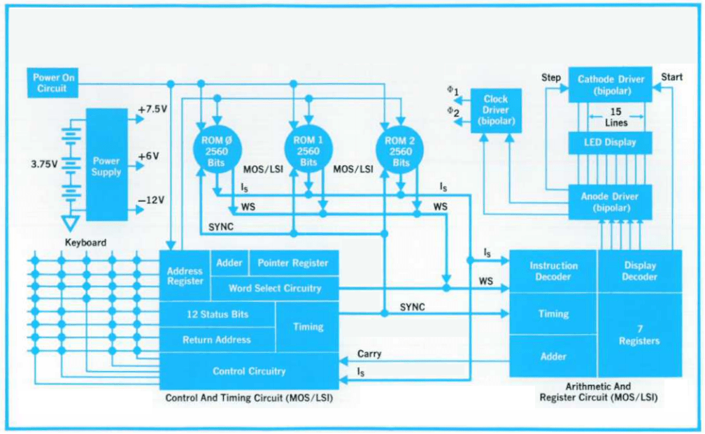
It was obvious from the start that testing different ROMs required a programmable tester compatible with rapid updates. There were unusual requirements compared to the way microcomputers and microprocessors work today. To keep power dissipation low, the HP-35 calculator ran at only 200 Khz — and it was a serial computer, not parallel like today’s chips. That digit-serial, bit-serial organization reduced package size and costs, and increased reliability.
This set a requirement that the new tester had to run at 200 KHz speeds and be programmable. Moreover, because the HP family was well thought out in advance (and Mostek needed better testers), the engineers chose one of the first PDP-11 microcomputers and its Unibus system which could run at megahertz speeds.
That became the basis for the Bluebird tester.
The Bluebird was originally designed to test the HP-35 “West Coast” calculator chips but were general purpose and used for the entire HP family of HP-35, HP-45 and other calculator parts — and for “random logic chips,” which at Mostek meant “not RAM.”
RAM chips required much more extensive tests.
The “West Coast” was named as such because HP was on the West Coast, while we were in Carrollton, Texas. The first machine went live in February 1972. Around 20 of these were built during my stay there.
This custom test system was also the first computer-controlled IC test system at Mostek. All other testers before then were digital state machines we called “dedicated testers” controlled by logic gates, counters, and in the case of some calculators, by an endless loop paper tape reader. We made small DRAMs, too, and tested them with dedicated testers with rows of potentiometers to set up the critical time. None of the dedicated testers had a CPU.

New tests
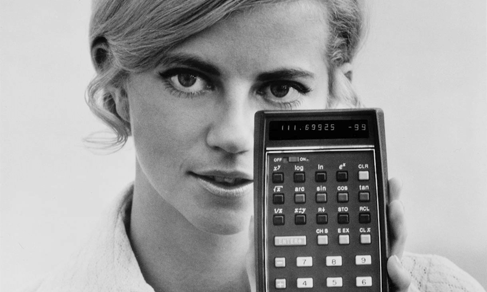
All parts from then onward had to be hand tested in a hacked HP-35 calculator that did a simple “reset” test and a 1+2 test. It worked something like this: First, the display showed 2, then a 3, and the chip would reset. It then showed 1, 2 and then a 3. If the final 3 happened, the test passed.
I found out many years later that Mostek had put in special mask “cheats” to prevent people from copying our chip. Mostek co-founder and chief designer Robert Proebsting had discovered a way to put a pad on top of a silicon hill, but without connecting it to the obvious trace below. A copier would be unable to see this hill that served as an insulator unless they used a side-viewing microscope, which was rarely used. Copying was almost always done with a top-illuminated microscope.
That would throw off a copier who’d think it was just an ordinary via, and connect the trace to the layer below. This chip had a circuit to signal the specific 2+3 operation, and this would then be connected by the wrongly copied pad to the reset pin of the chip.
That test set would be to just press 2, Enter (it was a reverse Polish calculator), a 3, and then +. This would reset the chip. Next, the test called to press 1, Enter, 2, and +, displaying a 3. If the chip was from AMI, or a bad chip, a different pattern would appear.
But since every test and logic circuit in the Bluebird in turn had to be tested, a special test program and circuit was created just to test… the Bluebird.
Mostek also hired more QC people and their diligence required tests for every lot of parts before and after setting up a test. I met my future wife because of that incident — she was one of the new QC personnel they hired for the increased workload for this production area. That was 44 years ago and we have been together ever since.
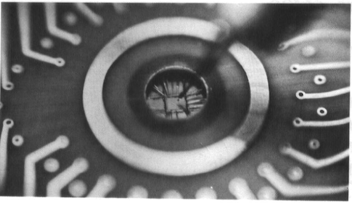
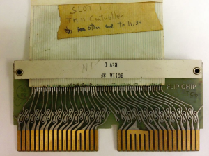
But since every test and logic circuit in the Bluebird in turn had to be tested, a special test program and circuit was created just to test… the Bluebird. The lid was raised up to access the test board which held various circuits specific to each IC. There was a hole in the lid, just to the upper left, where the Device Under Test (DUT) would be placed into a test jig on top of the test board.
There were two drawers of logic in the Bluebird. The bottom held three rows of logic to interface to the PDP-11. The top drawer held analog circuits, such as level shifters and D/A converters. The very expensive sets of 12-bit D/A converters (from 1970, when the system was first designed) were plugged into card slots in the top rack.
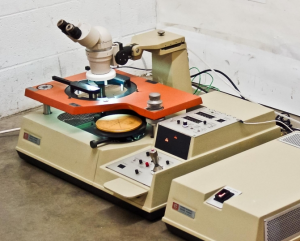
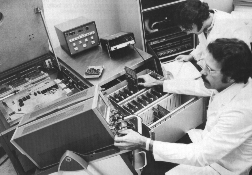
Bluebirds also ran Mostek’s wafer-level probe tests on the raw wafers. An Electroglas wafer prober would be set on top of this lid, and a cable ran through the hole to the test point card in the Electroglas. The tests for leakage and speed would be reduced when testing bare die by the PDP-11.
The Bluebird had 24 output bits that could be changed on-the fly by setting memory in the PDP-11 with 1’s and 0’s. This was done by writing a 15-bit start address and length into a Bluebird register, writing a test destination address into another register, and then enabling the tester. The logic circuits would automatically request a 16-bit memory address, write the data to a temporary register, read the next 8-bit byte, and write the resulting 24 bits to the DUT when the timing generator indicated it was time to do so.
We referred to this as “cycle stealing” from the PDP-11. These bits would travel through level translators to be at the correct PMOS levels. Other TTL compatible chips could be tested by reprogramming the DACs that drove the level shifter.
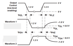
We did not just drive the signals from rail to rail either. We had to drive them between the Min and Max, and at the correct rise and fall times. Every data sheet value and waveforms had to be tested. For a TTL part, these input levels would be typically set at 0.8 volts to +2.4 volts with Vcc set to Max of +5.5 V. The parts had to always see a worst-case input. We also measured the input capacitance, which was difficult to do at the end of a long cable. Leakage current was tested, and we also back-biased the inputs to check that the anti-static protection diodes were working.
All the level shifters and analog circuits had to be custom designed for this purpose. We used standardized wire-wrap cards with small plastic headers to hold the discrete transistors and resistors that made up a level translator or a comparator.
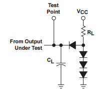
Another requirement is that the Hewlett-Packard chips had to meet worst-case output levels. If the part was supposed to drive an output to 0.4 volts at -4 ma, and 2.4 volts high to +3 ma, we had to test for exactly that. This required a bank of comparators (the Bluebird had 16) and suitable voltage sources and test loads, like the circuit at the right, to compare against.
The timing generators would strobe the comparator banks and write the result data to the PDP-11 memory using a third DMA cycle.