We Picked Apart the Milestone HP-35 Calculator
Testing the original scientific pocket calculator with Mostek's Bluebird
by FRED BECKHUSEN
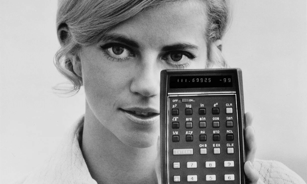
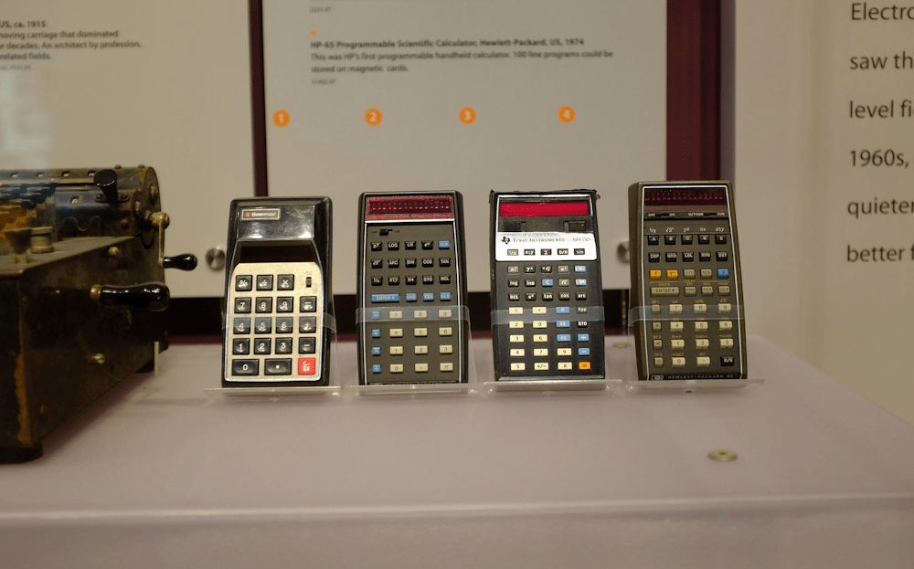
The HP-35 calculator was the first handheld, battery-powered scientific calculator. Introduced in 1972, the pocket computer sold for $395 and was an enormous success. Hewlett-Packard expected to sell 50,000 units but sold that amount in the first two months. General Electric snapped up 20,000 HP-35s just for internal use. Defying expectations, HP sold more than 300,000 of the venerable HP-35 calculators by 1975.
To put this in perspective, a $395 calculator costs the equivalent of $2,777 in today’s money, resulting in $840,000,000 in equivalent sales in just three years — and for only one model. HP continued to use the calculator’s chip sets and derivates of them for many years. Geeks loved them – and they have since traveled to the top of Mount Everest and into space. In 2009, the Institute of Electrical and Electronics Engineers honored it as a “Milestone in Electrical Engineering and Computing.”
I was awestruck reading about the HP-35 calculator that year and had no idea that I would soon work on them at an intimate level at the very company that designed and made the HP-35’s ICs. There is a lot of information online about this marvelous machine, but little about how it was manufactured, or how it was tested. I wish I had known back then what I know today – because I worked on the HP-35s, their chip set and architecture for a long time without even knowing it.
At the time, I was working for Mostek, which was racing to get a commanding market share of the world’s dynamic random-access memory (DRAM) chip market. The HP contract was the largest contract Mostek received for many years and not exceeded until Mostek developed the multiplexed DRAM, which took over the world.
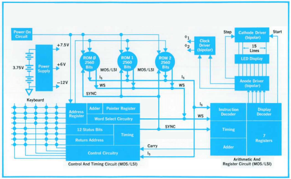
The Mostek contract required the custom design of three PMOS ICs, each with roughly 6,000 transistors. These were the MK6022, MK6023, and MK6024 ROMs — which differed only in the pattern loaded in them — together with the MK6021 Timing and Control IC, and MK6020 Arithmetic and Register chip. Together with the 1820-0853 anode driver and system clock chip, three 1820-0854 LED drivers, three LED 5-digit LED chips, and an 1820-0855 clock generator, they made up a small ROM-programmed computer.
The HP-35 used three ROM chips, with 768 10-bit instructions each. Each chip handled a “page” of memory, organized in banks of four, called “quads.” The HP-35 had 3/4 quad. Later HP calculators such as the HP-80 used as many as seven chips, and the chips were quadrupled in size to hold more data.
HP series of calculators and memory sizes:
| Model | Instructions | Quads (1 quad = 1024 instructions or 4 pages of 256 instructions) | |
| HP | 35 | 768 instructions | 3/4 quad (3 pages of 256 instructions each) |
| HP | 45 | 2048 instructions | 2 quads |
| HP | 80 | 2048 instructions | 2 quads |
| HP | 65 | 3072 instructions | 3 quads |
| HP | 70 | 2048 instructions | 2 quads |
| HP | 55 | 3072 instructions | 3 quads |
| HP | 19C | 5120 instructions | 5 quads |
| HP | 10 | 1536 instructions | 1 1/2 quads |
| HP | 21 | 1024 instructions | 1 quad |
| HP | 25 | 2048 instructions | 2 quads |
| HP | 22 | 2048 instructions | 2 quads |
| HP | 91 | 3072 instructions | 3 quads |
| HP | 29C | 4096 instructions | 4 quads |
| HP | 27 | 3072 instructions | 3 quads |
| HP | 25C | 2048 instructions | 2 quads |
| HP | 67 | 5120 instructions | 5 quads |
| HP | 97 | 6144 instructions | 6 quads |
| HP | 92 | 6144 instructions | 6 quads |
The chipset could address eight ROMs, but never used more than five, because the chips were quadrupled up in size, thus leaving only a single spare memory bank of 256 instructions.
Each chip had features that were about 10 microns (0.0004 inch) on a side, enormous compared with modern versions, about 2000 of which would fit inside each one.
Back at Mostek, engineers with their new HP-35s soon took to unsoldering the ROMs and replacing them with HP-45 chips as an upgrade. This was possible because the HP-35 calculator had two Quad chips. The only other difference was in the mask patterns and more keys in the HP-45, accessed with a shift key that created alternative functions. The test data that came from the calculator’s CPU also needed to vary from part to part.
Eventually, the engineers made 24 different parts for 13 different HP calculators.
| Type | Year | Function | Calculator | Comments |
| HP65-CPU | 1973 | Programmable Scientific | HP-65 | Hybrid CPU-module |
| MK6111 | 1973 | ROM | HP-65 | ROM#1 |
| MK6112 | 1973 | ROM | HP-65 | ROM#2 |
| MK6113 | 1973 | ROM | HP-65 | ROM#3 |
| MK6020 | 1972 | Arithmetic Chip | HP-35, HP-45, HP-55, HP-70 | |
| MK6021 | 1972 | Control and Timing Chip | HP-35 | |
| MK6022 | 1972 | ROM 256*10 bits | HP-35 | ROM#1 |
| MK6023 | 1972 | ROM 256*10 bits | HP-35 | ROM#2 |
| MK6024 | 1972 | ROM 256*10 bits | HP-35 | ROM#3 |
| MK6036 | 1973 | RAM 10*56 bits | HP-45, HP-55, HP-70 | |
| MK6134 | 1973 | ROM 1024*10 bits | HP-55 | |
| MK6215 | 1974 | Arithmetic Chip | HP-22, HP-25, HP-25C | |
| MK6216 | 1974 | Arithmetic Chip | HP-29C, HP95C, HP-97 | |
| MK6217 | 1974 | Arithmetic Chip | HP-21 | |
| MK6220 | 1974 | RAM 16*56 bits | HP-22, HP-25 | |
| MK6250 | 1975 | Card Reader Control | HP-67, HP-97 | |
| MK60038 | 1975 | ROM | HP-67 | added Anode drivers |
| MK60126 | 1975 | ROM | HP-25, HP-25C | |
| MK60142 | 1975 | ROM | HP-19C | |
| MK60171 | 1975 | ROM/RAM | HP-67, HP-97 | |
| MK60172 | 1975 | ROM/RAM | HP-67, HP-97 | |
| MK60175 | 1975 | ROM/RAM | HP-67 | |
| MK60176 | 1975 | ROM/RAM | HP-67 | |
| MK60185 | 1975 | ROM/RAM | HP-19C, HP-29C |
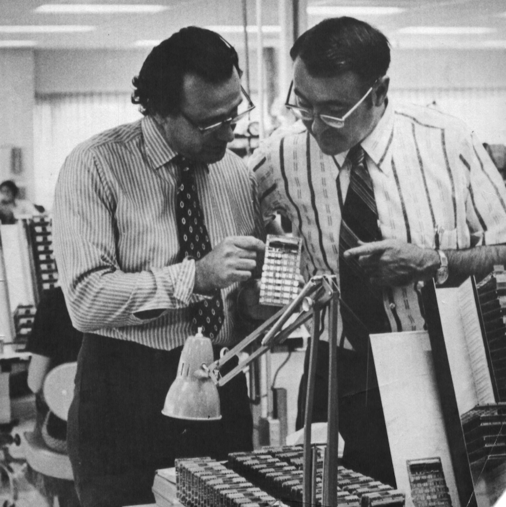
As a technician who knew how to solder, these DIY calculator experiments were quite a thrill.
Enter the Bluebird
It was obvious from the start that testing different ROMs required a programmable tester compatible with rapid updates. There were unusual requirements compared to the way microcomputers and microprocessors work today. To keep power dissipation low, the HP-35 calculator ran at only 200 Khz — and it was a serial computer, not parallel like today’s chips. That digit-serial, bit-serial organization reduced package size and costs, and increased reliability.
This set a requirement that the new tester had to run at 200 KHz speeds and be programmable. Moreover, because the HP family was well thought out in advance (and Mostek needed better testers), the engineers chose one of the first PDP-11 microcomputers and its Unibus system which could run at megahertz speeds.
That became the basis for the Bluebird tester.
The Bluebird was originally designed to test the HP-35 “West Coast” calculator chips but were general purpose and used for the entire HP family of HP-35, HP-45 and other calculator parts — and for “random logic chips,” which at Mostek meant “not RAM.”
RAM chips required much more extensive tests.
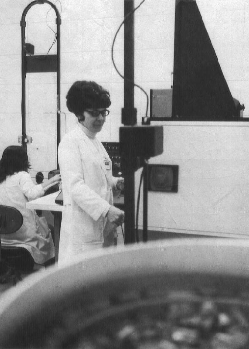
The “West Coast” was named as such because HP was on the West Coast, while we were in Carrollton, Texas. The first machine went live in February 1972. Around 20 of these were built during my stay there.
This custom test system was also the first computer-controlled IC test system at Mostek. All other testers before then were digital state machines we called “dedicated testers” controlled by logic gates, counters, and in the case of some calculators, by an endless loop paper tape reader. We made small DRAMs, too, and tested them with dedicated testers with rows of potentiometers to set up the critical time. None of the dedicated testers had a CPU.
How it worked
Programming the Bluebird involved hand-keying in a bootstrap loader into the PDP-11’s switch register, then loading an “absolute loader” tape with the bootstrap, which loaded the test program. We needed more speed and more RAM, so Mostek designed a custom RAM memory board. And every time we had a power failure, the other technicians and I would run around as fast as we could, re-keying in the bootstrap loader and loading the tapes again. This happened too often early on Sunday mornings.
I keyed in that bootstrap so often, I still remember the beginning of the bootstrap, 42 years later.
012737   move.w #1, #164162  // Put 1 in the Bluebird Online register
000001
164162
000002   Wait for Interrupt
....
At this time, the Bluebird would signal an interrupt over the Unibus cable.
The Unibus was a 120-ohm impedance-controlled flat cable that memory mapped the Bluebird into the PDP-11’s 32K word address space — much like any computer bus in use today. It ran through the PDP-11, but also was extendable by a long, flat impedance-controlled cable to external devices. The closest analogy to the Unibus architecture is perhaps the MK68000 chipset as the 68K was largely inspired by the PDP-11. The Unibus had an 18-bit address and 16 bits of data, plus two parity bits, one for each byte.
More importantly, there was a Master Sync that would clock the addresses (much like the 68K Address Strobe pin) and going the other way was Slave Sync (like DTACK on the 68K). This let Mostek designers create registers inside the Bluebird. It also had a Non Processor Request (DMA) pin for requesting and a NPG (Bus Grant) pin for granting a DMA cycle, and four interrupts. The Bluebird used these signals and the Unibus to DMA signals to and from the HP35 ICs as part of the test.
The Bluebird set me up for a surprise.
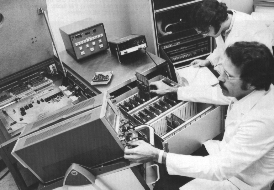
The Bluebird tester had two drawers of digital logic. The bottom drawer held the circuits for interfacing to the Unibus, and via it, access to the PDP-11 memory. Then the data for stimulating the parts came from the PDP-11 memory via DMA over the Unibus.
I had worked on dedicated testers during my first few months at Mostek. On a dedicated tester, you triggered an oscilloscope probe with the “fail lamp” driver and used a second probe to look at the IC under test pins, the level translators, comparators, and so on until you traced your way back to the test inputs to find the problem. There could be a pin loose in a socket, or a blown circuit in a level translator. The triggered scope would discover the exact instant the test failed.
Bluebird Specification | Value |
Clock rate | 200 kHz |
Test vector to DUT | 24 bits |
Test vector to CPU | 16 bits |
Pattern memory | via DMA |
DC precision | 12 bits |
The Bluebird set me up for a surprise. The first time I tried this “trigger on the fail lamp” technique on the Bluebird, I connected the scope to the latch, and traced my way backwards to the lower digital drawer. I then realized I was tracing a signal all the way back to the Unibus, chasing after the Master Sync signal that indicated the program had just executed a move opcode to write a data bit into a register in the Bluebird that toggled on the fail lamp.
Later that night, it became clear that the only way to figure out the problem was to learn the programming of the CPU — which led later to my career as a designer and programmer for Unix systems and many microprocessors. Unix originally ran on Dec PDP hardware, and also was used back then on the 68000 microcomputer that Mostek made.
AMI was also selected as a vendor and designed a similar set of three ICs. The goal was to achieve 250 mW of power dissipation. But a comparison of the size and power dissipation of the chips from Mostek and AMI shows the Mostek IC as considerably lower in power — which meant the batteries could easily run for several times the four-hour requirement.
Circuit Type | AMI | Mostek | |
MK6022,23, & 24 | Instruction ROM (256X10): | 116 x 108 | 126 x 134 |
MK6020 | Arithmetic and Register: | 138 x 167 | 156 x 200 |
MK6021 | Timing and Control: | 163 x 169 | 150 x 212 |
Power Used: | 100-120 mw | 73 mw | |
Size: | 63,121 sq mils | 79,882 sq mils |
The CPU instruction word was 10 bits, but to save on chip size, the parts were based on serial data. The 10 bits were clocked out, one at a time, and all calculations were done by a half-adder inside the Arithmetic and Register (A&R) chip. This feature of the chip required a word select line from the Control and Timing chip to signal to the A&R chip when the appropriate digit was available.
There was also a SYNC pin that signaled the beginning of an instruction word. This signal went to a special card in the Bluebird tester which we called by its secret code name: the “West Coast Sync” board.
Secret chip
Only a few people at Mostek had any idea these chips were for an HP calculator. It was a carefully kept secret. The code name was used whenever possible — even in the schematics for the tester.
One day, I worked on a Bluebird that was repeatedly failing a test. I was getting nowhere — stuck deep inside the digital logic on the “WC Sync” board. I asked several engineers what it was about, and they told me to just fix it. Eventually, a sympathetic engineer who realized I had a “need to know” told me the chips were for the HP-35 calculator, and how the “West Coast Sync” really worked.
That was a bit shocking — the HP-35 calculator was famous.
But now it made sense. From the calculator’s perspective, a timing circuit on each ROM was synchronized to the trailing edge of the SYNC signal issued by the Control & Timing chip when the calculator was turned on. This circuit then kept the ROM chip running synchronously with the rest of the system.
The CPU and the DUT also needed to be in phase with each other so that the bit patterns matched just like inside the calculator. The “West Coast Sync” board would stop the DMA until the SYNC and Word Select pins were at a known state on the DUT. The clocks would then be in sync. Now each output could be compared to the PDP-11 registers’ expected output with a LM311 comparator IC.
The comparator IC was also strobed by the Bluebird clock to compare the two chips at the correct time. That IC failed on one of the test boards, and always produced an “OK” signal. No one detected the problem, and Mostek shipped a large batch of defective parts to Hewlett-Packard.
It caused a huge ruckus, and everybody was upset.
New tests
All parts from then onward had to be hand tested in a hacked HP-35 calculator that did a simple “reset” test and a 1+2 test. It worked something like this: First, the display showed 2, then a 3, and the chip would reset. It then showed 1, 2 and then a 3. If the final 3 happened, the test passed.
I found out many years later that Mostek had put in special mask “cheats” to prevent people from copying our chip. Mostek co-founder and chief designer Robert Proebsting had discovered a way to put a pad on top of a silicon hill, but without connecting it to the obvious trace below. A copier would be unable to see this hill that served as an insulator unless they used a side-viewing microscope, which was rarely used. Copying was almost always done with a top-illuminated microscope.
That would throw off a copier who’d think it was just an ordinary via, and connect the trace to the layer below. This chip had a circuit to signal the specific 2+3 operation, and this would then be connected by the wrongly copied pad to the reset pin of the chip.
That test set would be to just press 2, Enter (it was a reverse Polish calculator), a 3, and then +. This would reset the chip. Next, the test called to press 1, Enter, 2, and +, displaying a 3. If the chip was from AMI, or a bad chip, a different pattern would appear.
But since every test and logic circuit in the Bluebird in turn had to be tested, a special test program and circuit was created just to test… the Bluebird.
Mostek also hired more QC people and their diligence required tests for every lot of parts before and after setting up a test. I met my future wife because of that incident — she was one of the new QC personnel they hired for the increased workload for this production area. That was 44 years ago and we have been together ever since.
But since every test and logic circuit in the Bluebird in turn had to be tested, a special test program and circuit was created just to test… the Bluebird. The lid was raised up to access the test board which held various circuits specific to each IC. There was a hole in the lid, just to the upper left, where the Device Under Test (DUT) would be placed into a test jig on top of the test board.
There were two drawers of logic in the Bluebird. The bottom held three rows of logic to interface to the PDP-11. The top drawer held analog circuits, such as level shifters and D/A converters. The very expensive sets of 12-bit D/A converters (from 1970, when the system was first designed) were plugged into card slots in the top rack.
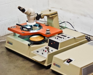
Bluebirds also ran Mostek’s wafer-level probe tests on the raw wafers. An Electroglas wafer prober would be set on top of this lid, and a cable ran through the hole to the test point card in the Electroglas. The tests for leakage and speed would be reduced when testing bare die by the PDP-11.
The Bluebird had 24 output bits that could be changed on-the fly by setting memory in the PDP-11 with 1’s and 0’s. This was done by writing a 15-bit start address and length into a Bluebird register, writing a test destination address into another register, and then enabling the tester. The logic circuits would automatically request a 16-bit memory address, write the data to a temporary register, read the next 8-bit byte, and write the resulting 24 bits to the DUT when the timing generator indicated it was time to do so.
We referred to this as “cycle stealing” from the PDP-11. These bits would travel through level translators to be at the correct PMOS levels. Other TTL compatible chips could be tested by reprogramming the DACs that drove the level shifter.
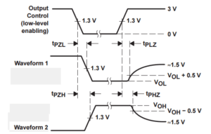
We did not just drive the signals from rail to rail either. We had to drive them between the Min and Max, and at the correct rise and fall times. Every data sheet value and waveforms had to be tested. For a TTL part, these input levels would be typically set at 0.8 volts to +2.4 volts with Vcc set to Max of +5.5 V. The parts had to always see a worst-case input. We also measured the input capacitance, which was difficult to do at the end of a long cable. Leakage current was tested, and we also back-biased the inputs to check that the anti-static protection diodes were working.
All the level shifters and analog circuits had to be custom designed for this purpose. We used standardized wire-wrap cards with small plastic headers to hold the discrete transistors and resistors that made up a level translator or a comparator.
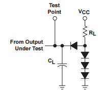
Another requirement is that the Hewlett-Packard chips had to meet worst-case output levels. If the part was supposed to drive an output to 0.4 volts at -4 ma, and 2.4 volts high to +3 ma, we had to test for exactly that. This required a bank of comparators (the Bluebird had 16) and suitable voltage sources and test loads, like the circuit at the right, to compare against.
The timing generators would strobe the comparator banks and write the result data to the PDP-11 memory using a third DMA cycle.
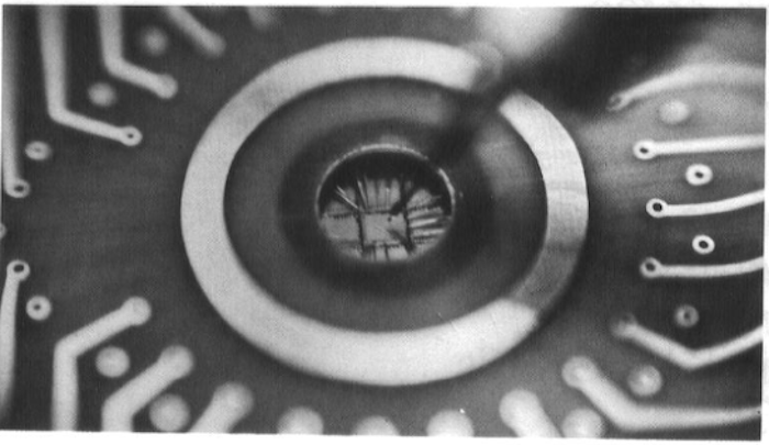
A three-inch wafer would be loaded into an Electroglas and aligned under a microscope. The test person would press start, and the Electroglas would step across the chip and press a set of microscopic probes attached to the PCB (above — with a circular hole in it). The blurry part that looks like a pencil was an ordinary medical syringe, filled with ink. It had a plastic fishing line running through it.
If the part failed the test, the Bluebird would enable the solenoid, which would push the fishing line, and jot a blob of ink onto the part. The wafer would be sent to the dicing department which scored and broke the wafer into individual parts and discarded the inked bits. The rest would go to the bonding and packaging department and get routed back to another Bluebird line for testing in the DIP package. In some cases, the parts would go through a heat or chill cycle in a large oven attached to another row of Bluebirds.
This cheap and effective method of marking bad die sometimes led to interesting patterns on the wafer. I was once asked to check out a Bluebird that was passing almost every part on a wafer. This was usually a nightmare – if there was a flaw, this was a sign it was broken in a way that was not easily fixable. In this case, it was easy to see that only the parts at the edges of the round wafers that were cut by the round edge were failing the test. This was either continuity or leakage test, and not the functional test which usually meant that there was a problem in the logic of the tester that tested the functions of the circuits.
I eventually noticed that one wafer had a line of dots running across it that was a great clue. The tester was correctly failing functionally bad parts. Looking at that wafer under a special microscope showed a microscopic grain boundary in the silicon — and transistors do not work across a grain boundary. They require a single crystal of silicon. The product engineer for the part later told me it was a final run for a very old part, an MK1002 dual 128-bit shift register. These parts were now being built in a new class 100 clean room using modern equipment and methods, and so the yield was now close to 100 percent.
Then there was the blue “Bluebird” color which was… unpleasant to look at. We painted everything bright blue — not that it was our preference. All test equipment had to be that way. Rows and rows and rows of testers. Room after room.
A few weeks later, we got an actual memo. We ignored it.
A technician named Mike Chambers received permission to design and build a board-level tester for our test lab based on the Z80 chip we were making at the time. And since we were in charge, he ordered a more attractive burnt orange and beige rack for our new “Puma” — short for “Programmable Universal Maintenance Aid.” We figured we could get away with it as it was a test lab, not a production department, and we had a different set of bosses.
Eventually the tester rolled out and went online in our lab. Shortly afterwards, we received the word that the vice president who oversaw color was upset and wanted us to take it apart and paint it blue. We ignored him. A few weeks later, we got an actual memo. We ignored it. We figured no one would take an expensive machine like that apart. We were right, too. We came in on Monday morning, and the room was painted burnt orange and beige.
The Bluebird was a true workhorse of a tester. It lasted for many years and tested close to every IC Mostek made except for RAM and the microcomputers. RAMs were tested on the Master and MiniMaster product lines (gray cabinets) and CPU chips were tested on Fairchild Sentry 600 and 700 series machines (beige cabinets). Bluebirds received several upgrades over the next five years — the wire wrap boards were retired, printed circuit boards were hand-taped, and wire wrap was used only for the two backplanes. The tape readers in the PDP-11s were replaced with serial RS-232 lines running to a VAX-11-780. We designed and laid out a diode ROM board for the PDP-11s so keying in the bootstrap was no longer needed.
After five years of this type of work, I made a lateral transfer to the microcomputer department and helped the engineers design STD Bus, Euro card, and VME bus systems. After eight years I left Mostek and started a Unix microcomputer company based on STD Bus systems and the 68000 microprocessor.
I still work with Rex Brown at Micro Technology Services. Rex was employee #13 at Mostek, one of their best test equipment designers, and the person who hired me into the microcomputer department so many years ago. We worked on STD and VME busses together for several years and have hired each other back-and-forth at different companies for more than 40 years now. The HP-35 calculator is now part of history.
Fred Beckhusen is the founder and CEO of Micro Technology Services, Inc.
