// Contract Engineering Services
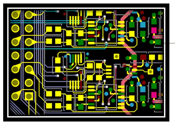
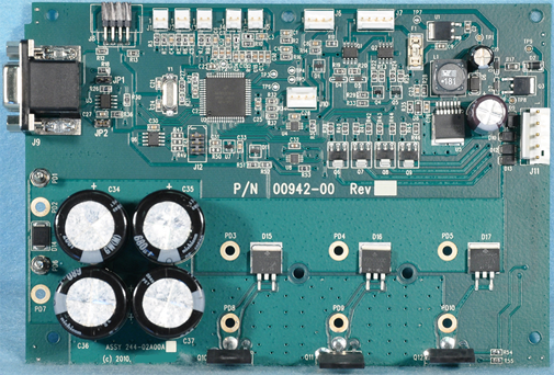
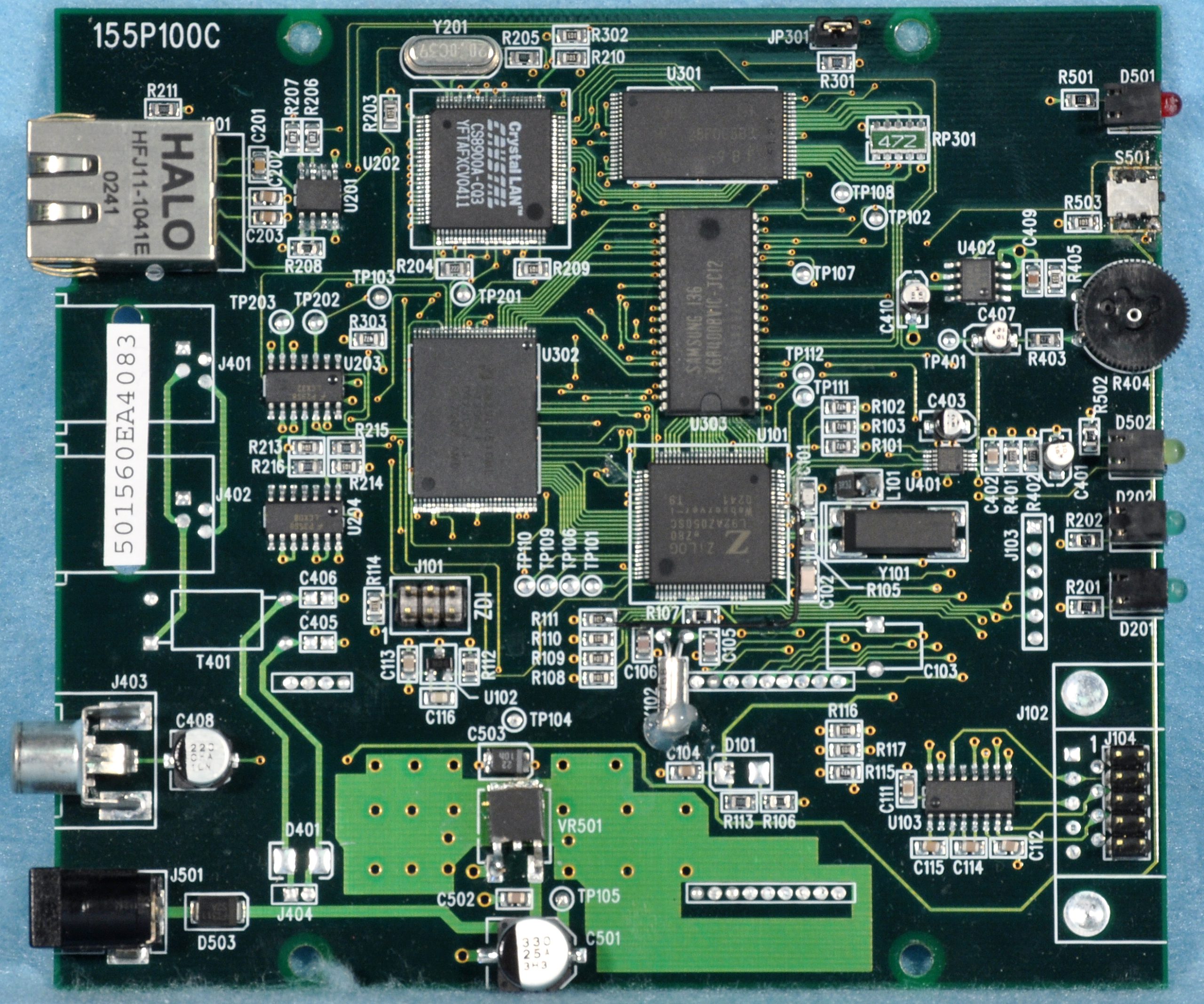
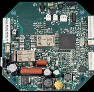
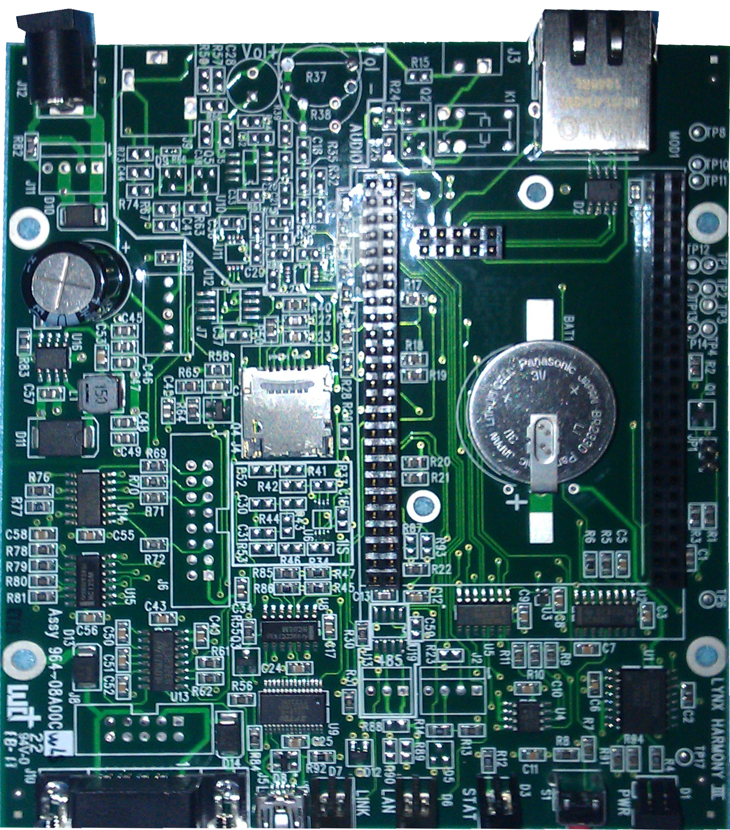
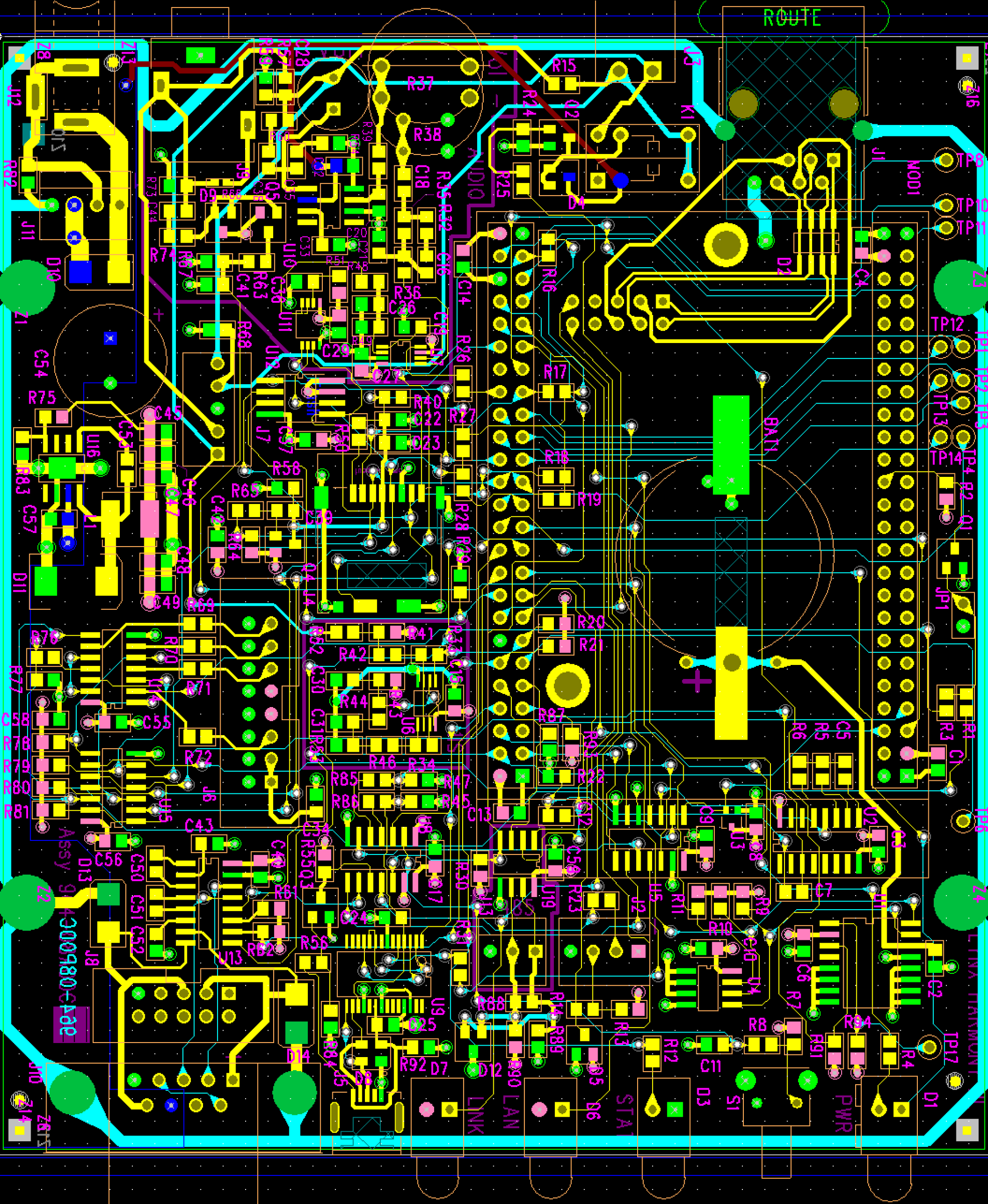
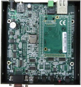
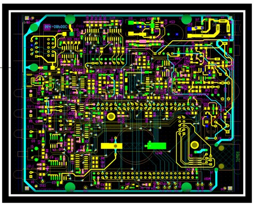
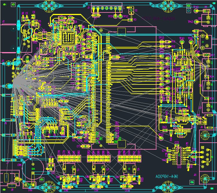
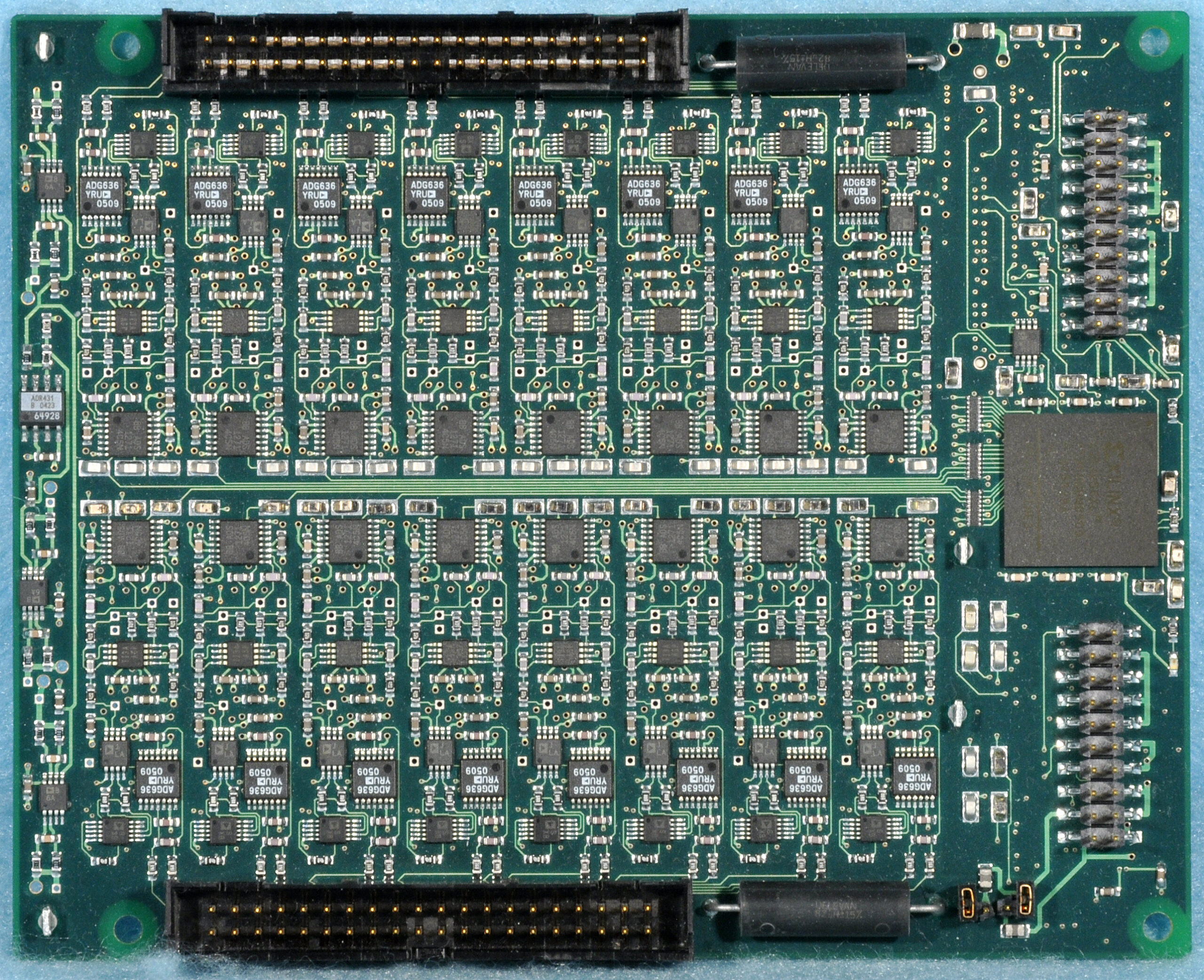
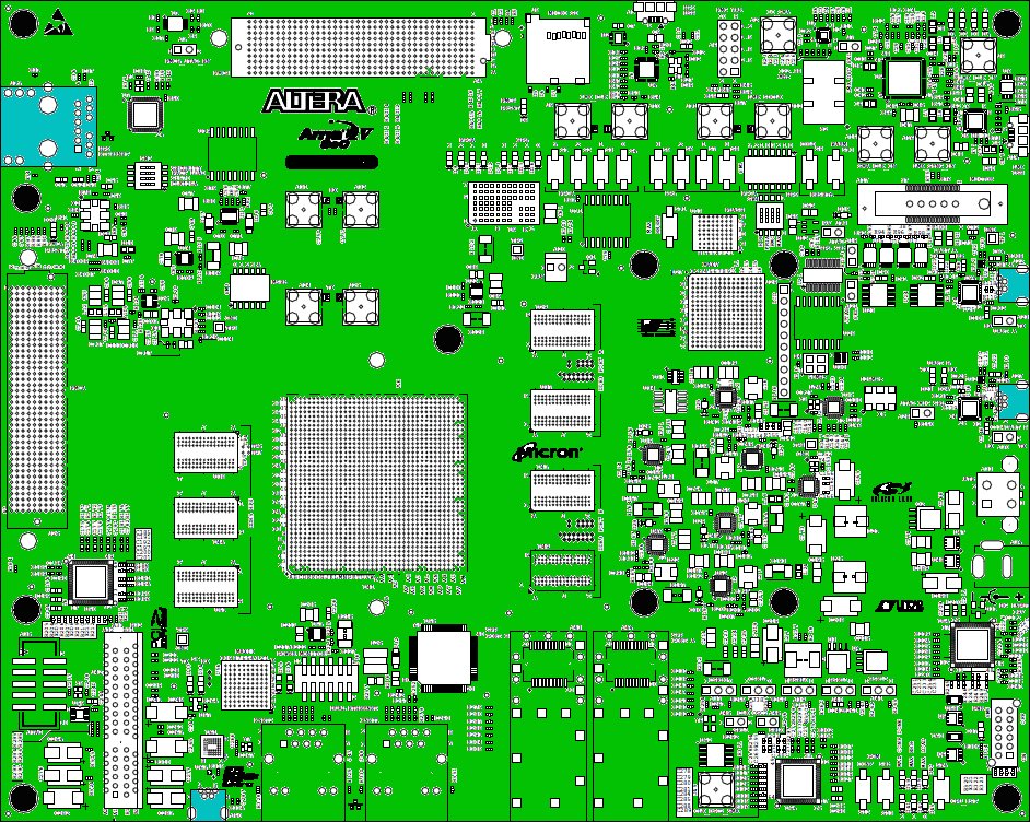
Custom PCB Design & Layout
We are fully qualified to work on the toughest and most challenging custom PCB design and layout jobs – and the easy ones, too. Custom PCB design is a complex and challenging task, but it is essential for the development of high-quality electronic devices.
MTSI meets the challenge with exceptional quality.
If your schematics include trade secrets or proprietary information, we will sign your non-disclosure agreements – or provide you with one of ours – to protect your intellectual property.
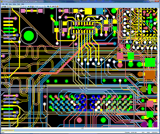
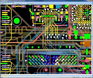
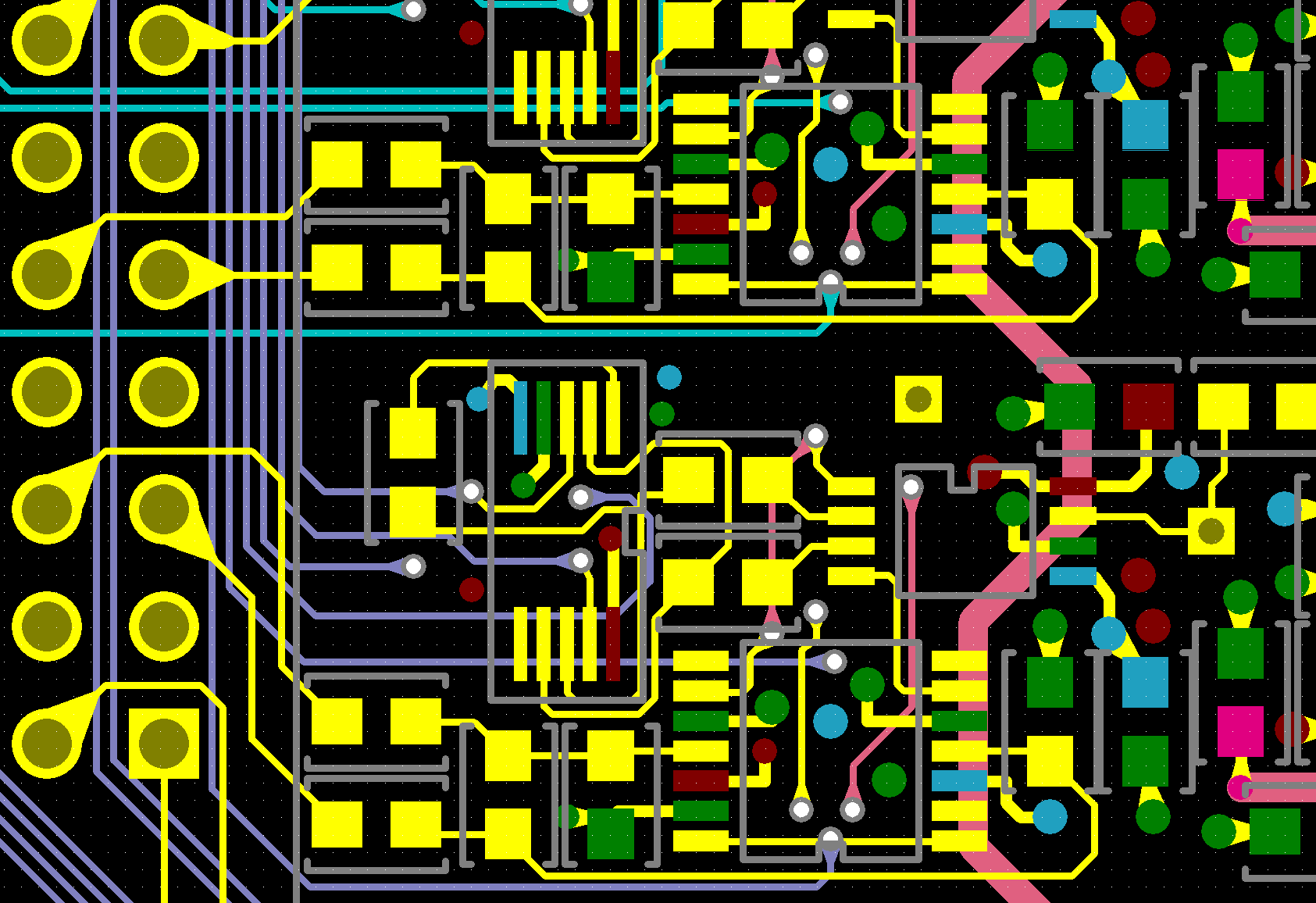
- PCB Layout
- Mentor PADS Accel Layout
- Schematic Entry
- Signal Integrity/Power Integrity