Dynamic random-access memory, or DRAM, is commonplace today in computers which use it to run their programs. They have high memory density and can pack a lot of data in a small space — and have fast access speeds and relatively cost effective. Back in the 1970s, Mostek was emerging as the world’s top DRAM manufacturer.
The first DRAM chip was made by Intel but Mostek developed a circuitry trick called address multiplexing.
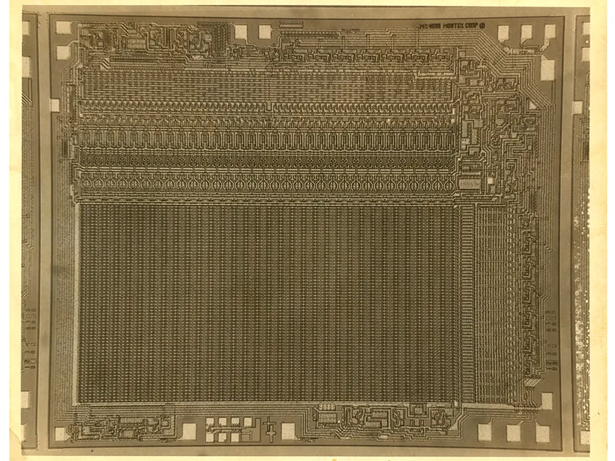
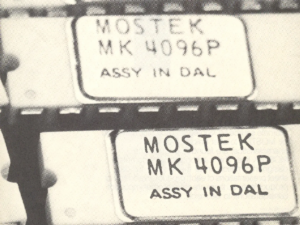
MTSI CEO Fred Beckhusen spoke with IEEE Spectrum about the innovative design — and the epic face-offs in DRAM history — when he was a recent hire drafted to test the Mostek MK4096P 4-kb DRAM with its 16 pins. This chip became the dominant DRAM for years, outpacing the 22-pin chips made by Texas Instruments, Intel and Motorola.
MTSI is now sharing this DRAM test Beckhusen wrote for the August 1979 edition of the Mostek Microcomputer Newsletter. The test ran on a 2.5-Mhz Z80. Reprinted below.
A tester could simply throw the CPU and card cage in a temperature chamber and let it run all morning — with some interesting and practical results. The test turns off the memory refresh by banging on the R (Refresh) register as fast as it could for one millisecond, then tested memory for any memory cells that discharged. If any bit failed, the test printed it.
The situation gets worse if combinations of wait states and bus acknowledges (DMA) are added. Add in the effects of higher temperature on refresh characteristics, and the system designer can no longer be confident that the Z80 will perform reliably in worst case conditions. Since possible combinations of #2, #3, and #4 are difficult to calculate, an alternative method of determining system performance is desirable.
The first of two programs presented are designed to quantitatively measure the refresh interval of dynamic RAM that uses the Z80 generated REFRESH signal. The program inhibits refresh for progressively longer periods of time by repeatedly loading the R register with 00 until memory fails. Because of this, the program must run in PROM or static RAM while testing. Any errors due to bits being dropped force the CPU to store the first failing address, data, and refresh period in memory locations ADDR (0002H), DATA (0004H), and TIME (000H).
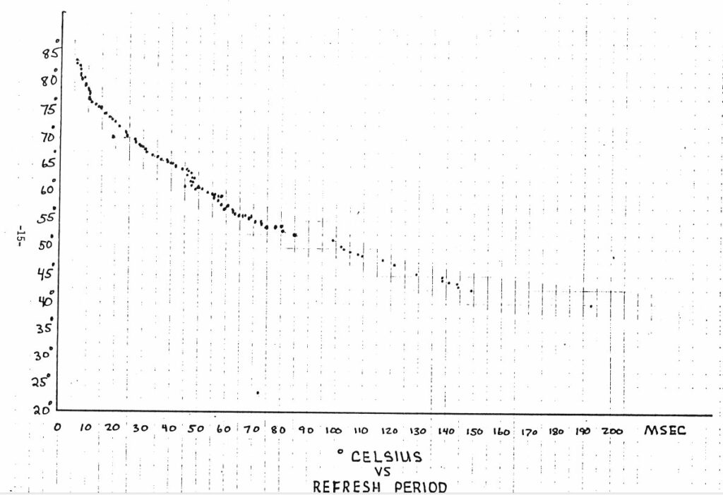
To test the program, a Mostek MDX system was heated in a test chamber and the resulting output of the program (X-AXIS) was plotted against the temperature (Y-AXIS) as shown in Figure 1. The system remained operational at 100 degrees C, but as the graph clearly shows, operation would not be reliable as the slope of the curve gets very steep at the higher temperatures.
Other system parameters affect Z80 system performance. With high temperature, bus drivers and receivers slow down, and RAM access times rise. All these degrade system performance. Compounding this problem on the Z80, opcode fetches, (M1 cycles) occur in 1/2 less clock cycles than normal memory read operations. This means that conventional store/read diagnostics cannot test a Z80 memory, either dynamic or static, at the memorys full access time requirement. For example, a 4 MHz Z80 will need memory data in 240 nanoseconds (worst case) during opcode fetches, but conventional Z80 memory diagnostic tests only require a 345 nanosecond access time (worst case. access time for a Z80 memory read cycle). This is similar to the 8080 problem where stack operations (push, pop) occur faster than normal memory references. Clearly, a good Z80 memory diagnostic must execute each memory location, fetching both 0’s and 1’s, and insure that the correct opcode was fetched (executed).
The second of the two programs executes every available memory location using four routines. The program tests 1/2 the memory for correct operation fetching 0’s, then the other half for 0’s, then two tests that check correct operation of each half fetching all 1’s. THe program sequentially generates the instructions. CB 00 and CB FF, RLC B and SET 7, A. As both bytes of these opcodes are fetched with an M1 cycle at the fast rate, half the memory will be tested for O’s or 1’s being correctly fetched. If opcodes other than RLC B and SET 7, A are fetched, then the B register will not be shifted or the A register will not have bit 7 set, and the program will halt, leaving the error address and error data in memory locations ADDR (0080H) and EXP (0092H).
Bibliography
1 Mostek Memory Data Book and Designers Guide. Jerry Winfield, pg. 280 1979
2 Mostek Microcomputer Data Book. pg. 154 1979